logo
Datasheet4U.com - RD74LVC1G79
logo

RD74LVC1G79 Datasheet, Flop, Renesas Technology

RD74LVC1G79 Datasheet, Flop, Renesas Technology

RD74LVC1G79

datasheet Download (Size : 2.03MB)

RD74LVC1G79 Datasheet
RD74LVC1G79

datasheet Download (Size : 2.03MB)

RD74LVC1G79 Datasheet

RD74LVC1G79 Features and benefits

RD74LVC1G79 Features and benefits

The basic gate function is lined up as Renesas uni logic series. Supply voltage range: 1.65 to 5.5 V Operating temperature range:
  –40 to +85°C All inputs:.

RD74LVC1G79 Description

RD74LVC1G79 Description

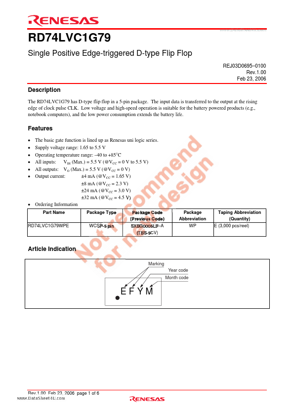
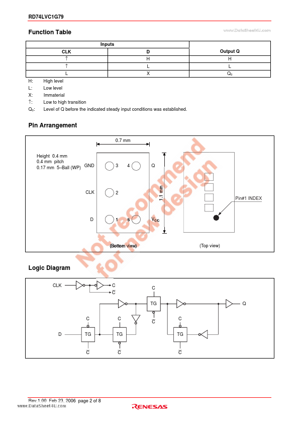
The RD74LVC1G79 has D-type flip flop in a 5-pin package. The input data is transferred to the output at the rising edge of clock pulse CLK. Low voltage and high-speed operation is suitable for the battery powered products (e.g., notebook computers), .

Image gallery

RD74LVC1G79 Page 1 RD74LVC1G79 Page 2 RD74LVC1G79 Page 3

TAGS

RD74LVC1G79
Single
Positive
Edge-triggered
D-type
Flip
Flop
Renesas Technology

Manufacturer


Renesas (https://www.renesas.com/) Technology

Related datasheet

RD74LVC1G00

RD74LVC1G02

RD74LVC1G04

RD74LVC1G07

RD74LVC1G08

RD74LVC1G125

RD74LVC1G126

RD74LVC1G14

RD74LVC1G17

RD74LVC1G240

RD74LVC1G32

RD74LVC1G86

RD74LVC1G98

Since 2006. D4U Semicon.   |   Datasheet4U.com   |   Contact Us   |   Privacy Policy   |   Purchase of parts